Ever wondered how your smartphone or smartwatch comes alive? At the heart of every modern gadget lies a PCBA, a Printed Circuit Board Assembly. It’s the key stage that transforms a plain circuit board into a functional tech brain.
In today’s digital age, every electronic device we use, be it a smartphone, smartwatch, or even your car key—contains one vital part: a Printed Circuit Board Assembly (PCBA). While a PCB is just a board with copper traces, a PCBA is the fully assembled version with all components placed and soldered—ready to power up.
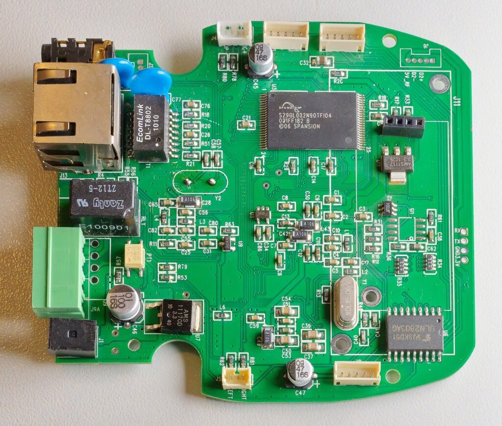
Below Image of Printed Circuit Board Assembly (PCBA): Loaded with Electronics Components.
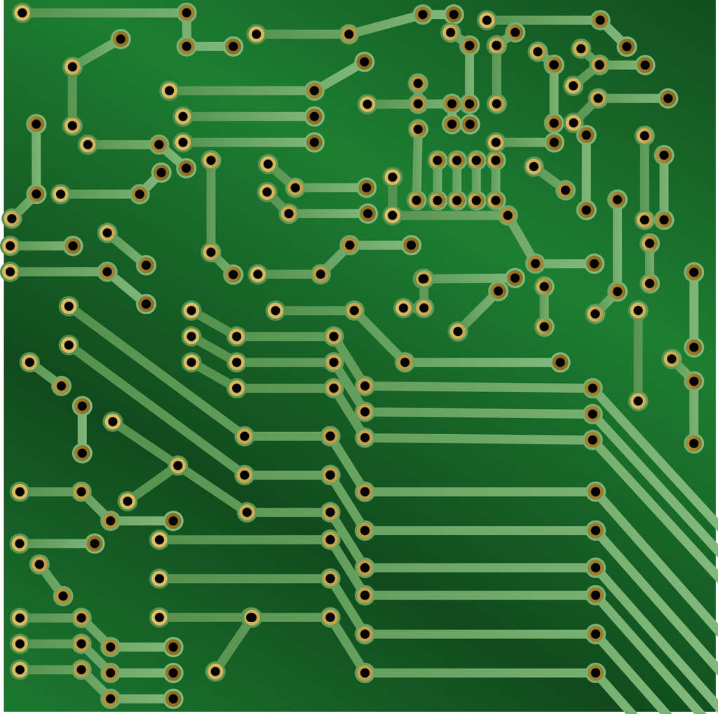
Below Image of Printed Circuit Board (PCB): Bare Board without Electronics Components.
Let’s break down how this essential process works, step by step.
Step 1: Prepping with Solder Paste Printing
The journey begins with solder paste application. A thin layer of this paste—made from powdered solder and flux is carefully deposited on selected pads of the blank PCB using a stencil. This sticky base holds components in place for the next step.
Step 2: Smart Component Placement
With the paste ready, it’s time to place the tiny components. Pick-and-place machines, controlled by software, mount everything from microchips to resistors with surgical precision. These machines can place thousands of parts every hour.
Step 3: Reflow Oven Magic
The loaded board enters a reflow oven, where it’s gradually heated. The solder paste melts, bonding each component to the board. Then it cools down, solidifying the connections.
This stage is used for Surface Mount Technology (SMT) parts.
Step 4: Automated Inspections
Next comes quality control. Specialized machines like:
- AOI (Automated Optical Inspection) visually verify placement.
- X-ray Inspection checks hidden joints, especially under complex chips like BGAs.
Defects are flagged immediately for correction.
Step 5: Adding Through-Hole Components
If the board design includes bigger components—like connectors or transformers—they’re manually inserted into pre-drilled holes. These parts can’t be mounted with paste and need a different method.
Step 6: Wave or Selective Soldering
The board is then passed over molten solder (in wave soldering) or receives solder at specific points (selective soldering) to secure through-hole components. This ensures strong mechanical and electrical contact.
Step 7: Functionality Tests
At this point, the board is almost done. Engineers test the PCBA using:
- In-Circuit Testing (ICT) for electrical accuracy
- Functional Testing to simulate real-world usage
- Firmware Loading, if the product requires software
Only the boards that pass every test move ahead.
Step 8: PCBA Cleaning Process
In some cases, leftover flux or contaminants are washed off using special cleaning agents. This is important for high-reliability electronics like medical or aerospace devices.
Step 9: Conformal Coating for Environmental Protection (Optional)
If the PCBA will be used in tough environments, a conformal coating or potting is applied. This protects against moisture, dust, and temperature extremes.
Step 10: Safe Packaging & Delivery
Finally, the board is sealed in ESD-protective packaging and gets ready for integration or shipment. From here, it could end up in a drone, wearable, or smart home gadget.
Summary
The PCBA manufacturing process is a mix of automation, precision, and human oversight. Whether it’s placing components with micron-level accuracy or testing for defects, each step ensures your tech works flawlessly.
Behind every electronic product is a hidden layer of engineering perfection.
DeepSeek vs. ChatGPT: Which AI Chatbot is Better? (2025 Comparison)
The Ultimate List of AI Productivity Tools You Need in 2025
The Most PROFITABLE YouTube Niches in 2025 (Proven!)
The Best YouTube Niches Nobody is Talking About (2025 Edition)