The bare Printed Circuit Board (PCB) is the foundational backbone of any electronic device. Before components are mounted through SMT or through-hole technology, the bare PCB must be precisely designed and fabricated. This article walks through each stage of the bare PCB manufacturing process, from the initial design phase to the final inspection, ensuring quality, performance, and reliability.
What is a Bare PCB?
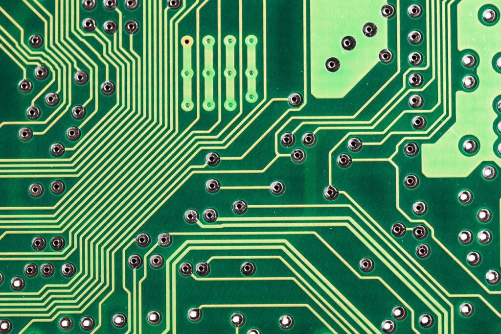
A bare PCB is a non-populated circuit board that contains only the conductive tracks, pads, and base material layers. It has no electronic components mounted on it. Its primary purpose is to provide the electrical interconnection between components using copper traces and vias.
Step-by-Step Process of Bare PCB Manufacturing
1. Design and Output (Gerber File Generation)
- PCB design starts with software like Altium, KiCAD, Eagle, or OrCAD.
- Designers generate Gerber files, which include data for:
- Copper layers (top/bottom)
- Solder mask
- Silkscreen
- Drill holes
- The Design Rule Check (DRC) ensures the layout meets manufacturing capabilities.
2. Material Selection and Cutting
- The base material, usually FR-4 (fiberglass epoxy laminate), is chosen based on performance needs.
- The large FR-4 sheets are cut into panel sizes ready for further processing.
3. Inner Layer Imaging (for Multilayer PCBs)
- A photoresist film is applied to the inner core layers.
- UV light exposure through the inner layer artwork hardens the required pattern.
- The unexposed areas are developed away, leaving behind the copper traces.
4. Etching the Inner Layers
- Chemical etching removes unwanted copper, leaving only the desired circuitry.
- This process is followed by resist stripping to reveal the clean inner copper traces.
5. Lamination (Layer Bonding)
- Inner layers, prepregs (insulating layers), and outer copper foils are stacked and pressed together under heat and pressure.
- This forms a solid multilayer PCB structure.
6. Drilling
- CNC drilling machines create precise holes (vias, component holes).
- Hole locations are guided by drill files from the Gerber data.
- High-density PCBs may also require laser drilling for microvias.
7. Desmearing and PTH (Plated Through Hole) Formation
- After drilling, smear and debris are cleaned.
- Through-holes are chemically plated with copper to enable electrical connectivity between layers.
8. Outer Layer Imaging
- And again photoresist is applied to the outer layers and then UV light transfers the outer copper circuit pattern.
- also Unwanted copper is etched away & leaving behind the outer layer traces.
9. Solder Mask Application
- A protective solder mask (usually green) is applied over the board.
- Openings are made for pads and vias where components will be soldered.
- This prevents short circuits and oxidation.
10. Silkscreen Printing
- Component labels, logos, and orientation marks are printed using white epoxy ink.
- The silkscreen helps with manual and automated assembly.
11. Surface Finish Application
To ensure solderability and prevent oxidation, surface finishes are applied. Common types include:
- HASL (Hot Air Solder Leveling) – Leaded or lead-free
- ENIG (Electroless Nickel Immersion Gold)
- OSP (Organic Solderability Preservative)
12. Electrical Testing
- Automated testing is done to ensure there are no shorts or open circuits.
- Flying probe or bed-of-nails testers validate the PCB’s electrical integrity.
13. Final Inspection and Quality Control
- Visual inspections, dimensional checks, and AOI (Automated Optical Inspection) are performed.
- Only boards meeting IPC Class 2 or Class 3 standards are passed for delivery.
Common Bare PCB Types
| Type | Description | Application |
|---|---|---|
| Single-sided | One copper layer | LED lights, toys |
| Double-sided | Copper on both sides | Consumer electronics |
| Multilayer | 4–50+ layers | Servers, medical, automotive |
| Rigid-flex | Combines rigid & flexible | Wearables, aerospace |
| High-frequency | PTFE-based | RF/microwave devices |
Conclusion
The bare PCB manufacturing process is a combination of chemical, mechanical, and thermal processes, all working in harmony to deliver precise and durable boards. Whether it’s a simple single-sided board or a complex multilayer stack-up, quality at every stage ensures performance, reliability, and manufacturability in the final product. Choosing the right manufacturing partner and understanding the process helps engineers and designers create better electronics with fewer failures and delays.
A Complete Guide to Solder Paste Types for Surface Mount Technology
What is End-to-End Encryption? You must know it.
https://multitechlove.com/category/ems
Types of PCBs Explained: A Complete Guide for Beginners
Simple Beginner’s Guide to the PCBA Manufacturing Process
FAQs on Bare PCB Manufacturing:
1. What materials are used in bare PCB manufacturing?
The most commonly used material is FR-4, a fiberglass-reinforced epoxy laminate. Other materials include polyimide (for high-temperature applications), PTFE (for RF/high-frequency), and aluminum (for LED and power electronics).
2. How many layers can a bare PCB have?
Bare PCBs can range from single-layer to multilayer boards with 50+ layers, depending on the complexity and application. Most consumer and industrial electronics use 2 to 8 layers.
3. What is the role of Gerber files in PCB manufacturing?
Gerber files contain all the necessary data for fabricating a PCB, such as copper layer layouts, drill holes, solder mask patterns, and silkscreen details. They act as the blueprint for the manufacturer.
4. What is the difference between a bare PCB and an assembled PCB?
A bare PCB includes only the board and copper traces. An assembled PCB (also called a PCBA) has all components soldered onto it and is ready for use in an electronic device.